


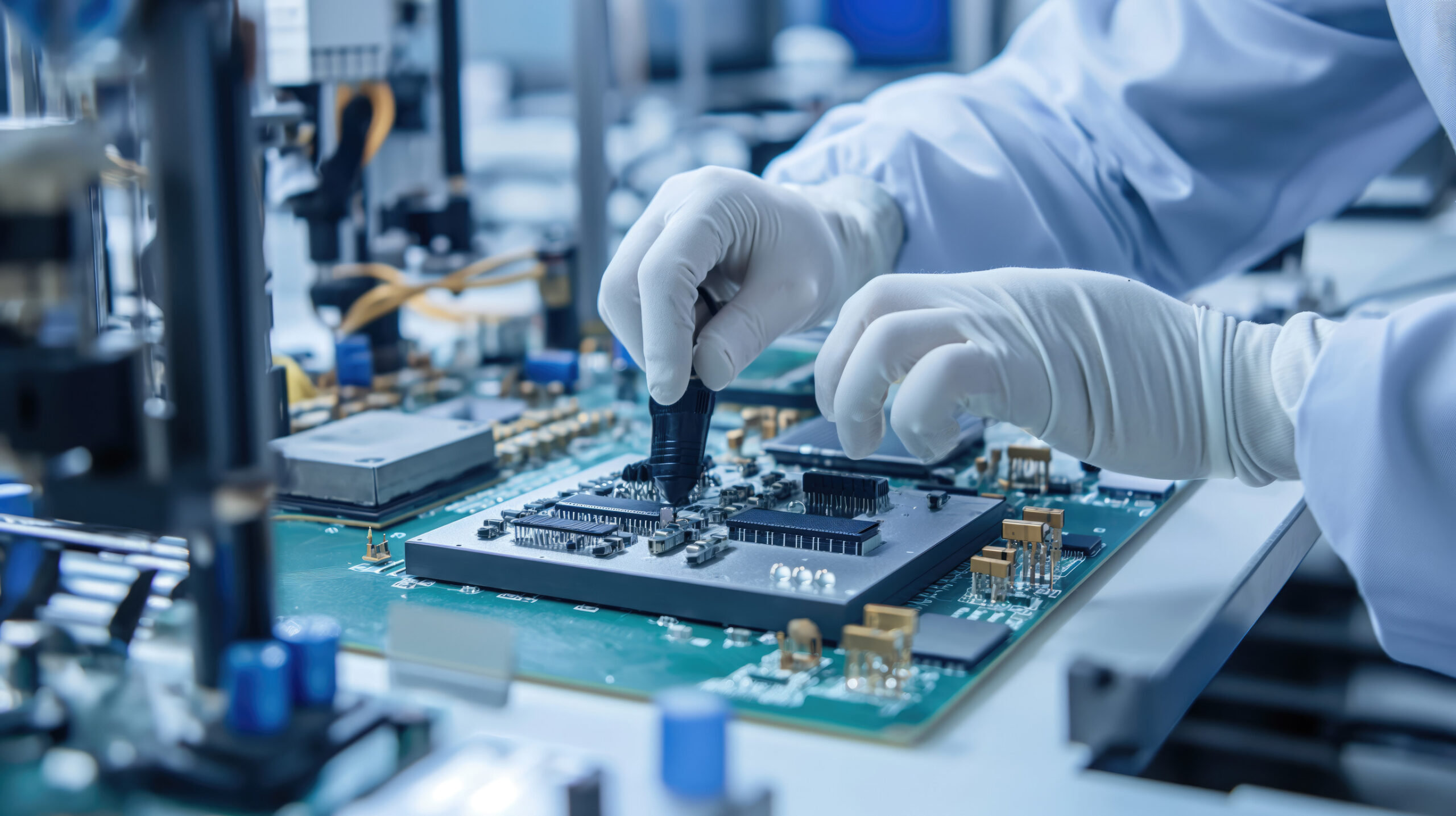
The assembly of a printed circuit board may seem to be a complicated puzzle. It can go wrong a lot with small parts, soldering, and circuit boards of low-level designs. Even a minor error will result in a board that is not functioning, and you will have to waste a lot of time in troubleshooting or even rebooting. It is essential whether you are a hobbyist a personal project or a professional developing a prototype that everything goes smoothly in the PCB assembly process. The write-up involves 6 simple tips and tricks that can aid you in assembling your PCBs more efficiently and with fewer mistakes. These best practices may help you to achieve better results in your work and make the whole process less stressful.
6 tips and tricks of easy PCB assembly
1. Organize your components
You should take time to organize the electronic parts before you even think about soldering. Prepare a clean and well-lit area, and prepare all your parts in a systematic way. Another way to do it is to print Bill of Materials (BOM) and collocate the components with part numbers. The use of small containers or component tray may help to avoid losing small parts. This is such a basic precaution that you will not go through the hassle of trying to identify a certain resistor or capacitor once you are in the assembly process.
2. Solder from the inside out
When you have to start soldering, begin with the smallest and the flattest components foremost. This typically consists of beginning with resistors, diodes and small ICs at the center of the board. The low-profile components are soldered so that you can have a flat and level surface to operate on. The parts can be installed in any order, but the installer would find it hard to solder the small parts to taller parts such as electrolytic capacitors or connectors which have to be installed first. Being able to begin inside and then work outward is also an assurance that you can easily get access and will not inadvertently destroy bigger parts.
3. Apply the right quantity of solder
The correct level of solder added is an art but one that can be learnt with practice. Excessively small solder may either create a weak or nonexistent electrical contact, a so-called cold joint. Excessive solder may cause solder bridges whereby solder will tend to connect two or more adjoining pins resulting in a short circuit. The purpose is to form a dirty streamlined cone-shaped joint. Preheat the pad and the element lead with your soldering iron a second or so, and then embed the solder to the connection, instead of the iron. The solder is expected to create a smooth flow around the pad & lead.
4. Check component alignment
A significant number of electronic parts are polarized, and they should be mounted in a particular direction to be operational. Some polarized components may be ruined by being installed backwards. Be attentive to the markings on the element and the PCB. Diodes are marked with a line that represents the cathode, electrolytic capacitors with a stripe representing the negative lead and integrated circuits with a dot or notch that represents pin 1. These indicators should always be checked against the silkscreen on your printed circuit board prior to soldering.
5. Remove your board when soldering
The flux can be a little corrosive overtime and even conductive, residue that is left on the board after soldering, and this results in long-term reliability problems. It also causes the board to appear disorganized and unprofessional. As soon as soldering is complete, rub the board softly with a small and stiff brush with a special flux cleaner or isopropyl alcohol. This would get rid of the sticky stuff and your solder joints will be clean, and your board will appear professional. It is also a lot easier to check a clean board against any issues that may be present.
6. Inspect your work
With a digital microscope or a magnifying glass, get a closer look at each solder joint. Search any possible problems, that is, cold joints, solder bridges, or damaged components. It is worthwhile to check your work in the process, which will save you a lot of time in the future. When putting together several boards it is sometimes more effective to do one step on all boards and then go to the next step and then make the final inspection of a complete product.
Conclusion
These are a few simple tips that can aid in your PCB assembly (PCBA) procedure. Some organization, proper technique and thorough inspection will assist you in coming up with the reliable and professional boards at all times. Understanding these basics is a good start and you will have the confidence of taking more complicated projects.

